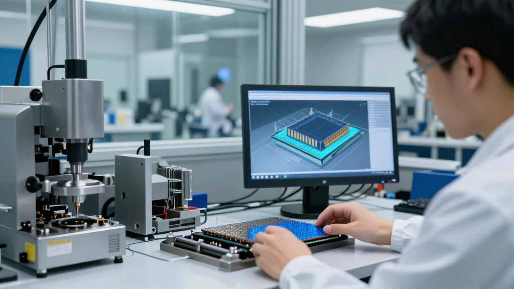
🔍 Read the full analysis: AI Chip Construction: A 3D Guide To Compute And Memory on ThorstenMeyerAI.com

Get the latest gadgets delivered free with Prime
- Fast, free delivery on millions of items
- Prime Video, Amazon Music and more included
- Member-only deals all year
TL;DR
ThorstenMeyerAI.com published a 3D explainer on November 22, 2026, showing how AI accelerators combine compute dies, stacked high-bandwidth memory, silicon interposers and liquid cooling. The report highlights memory bandwidth and advanced packaging as constraints on performance and production, while noting that the models use schematic dimensions.
ThorstenMeyerAI.com published a 3D explainer on November 22 showing how current AI accelerators combine compute dies, stacked high-bandwidth memory (HBM), silicon interposers and liquid cooling. The report argues that memory bandwidth and advanced packaging, not just compute capacity, shape accelerator performance and how many systems suppliers can build.
The guide breaks an accelerator package into its main physical layers: a package substrate for power and external signals; a silicon interposer that links compute chips and memory with dense wiring; compute dies; HBM stacks; and a cooling plate. The article says its open-source CAD models preserve the order and count of layers but use schematic dimensions. Nvidia and AMD do not publish the specific dimensions of the dies, package or memory stacks, it says.
The report compares several designs. It says Nvidia’s Rubin GPU uses two reticle-limited compute dies and cites Nvidia’s product page for memory bandwidth of 19.2 terabytes per second. AMD’s MI355X is described as using eight stacked accelerator complex dies, two I/O dies and eight 12-high memory stacks. Those configurations are reported by the source from company materials; they are not independent measurements.
HBM places DRAM chips in vertical stacks beside the compute dies, joined by through-silicon vias. The guide also describes the interposer and CoWoS packaging as a way to connect the components with more wiring than a conventional circuit board can provide. In a rack-scale example, Nvidia’s GB200 and GB300 NVL72 systems each have 72 GPUs and 36 CPUs, arranged across compute trays alongside NVLink switch trays and other rack equipment.
Memory and Packaging Set the Pace
The hardware layout matters because powerful compute dies need a steady flow of data. The source reports that Nvidia’s listed memory bandwidth rose from 900 GB/s for V100 to 19.2 TB/s for Rubin. Those figures refer to different products and are presented as a product comparison; the article’s broader point is that moving data can constrain how effectively an accelerator serves AI workloads.
Manufacturing capacity is another pressure point. Building the package requires joining large compute dies and multiple HBM stacks through advanced packaging, while rack-scale systems add requirements for liquid cooling, switches and power. The report cites SK hynix’s expectation that HBM demand will exceed supply through 2030. If that forecast holds, memory and packaging capacity could limit accelerator availability even as chipmakers expand compute capability. The source does not quantify how much those constraints affect prices or delivery schedules.
Popular right now

Bose QuietComfort Ultra Headphones Gen 1, Lunar Blue

Dyson V9 Motorbar Cordless Vacuum

KitchenAid Artisan 5-Qt Tilt-Head Stand Mixer, Almond Cream
As an affiliate, we earn on qualifying purchases.
From Chip Package to Rack
The guide places the package in a wider production timeline. It says TSMC’s CoWoS-S can accommodate an interposer up to about 2,700 square millimeters, or 3.3 times the area of a standard lithography reticle, citing the company. For larger packages, CoWoS-L uses silicon bridges in a carrier layer. The source says TSMC’s chief executive described five-reticle-size production as operating in the real world on October 15, 2026, with larger formats under development.
HBM stacks have also grown taller. The report cites the JEDEC HBM4 standard, published in April 2025, as allowing four-, eight-, 12- and 16-high stacks and up to 64 GB per stack. It also describes liquid cooling at rack scale: Nvidia specifies 120 kilowatts of cooling capacity for a GB200 NVL72 rack. These details show why an accelerator is not just a processor; its memory, packaging and surrounding infrastructure are part of the system.
“Where AI gets stuck today, it is often not the compute die. It is memory bandwidth, packaging, and how many of these parts the world can actually build.”
— ThorstenMeyerAI.com
Dimensions and Supply Remain Unclear
The article’s 3D models are schematic, not to scale. It says Nvidia and AMD do not publish the component dimensions needed to build dimensionally accurate package models, so the displayed sizes should not be treated as measurements. The report also relies on company product pages, technical documents and supplier statements for chip specifications and manufacturing claims.
The source does not establish the extent of any current shortage, how long individual customers may wait, or how much packaging constraints affect accelerator prices. SK hynix’s supply outlook is a company forecast, not a guarantee. The guide also does not provide an independent comparison of real-world performance across the named Nvidia and AMD products.
Watch Packaging and HBM Capacity
The next signals will come from manufacturers’ updates on HBM output and advanced packaging capacity, as well as product availability for rack-scale systems. TSMC’s stated work on interposers larger than five reticles and suppliers’ progress on taller HBM stacks will help indicate whether manufacturing can keep pace with accelerator designs. The source provides no specific release date or supply milestone beyond the announcements it cites.
Key Questions
What does the 3D guide explain?
It shows how an accelerator combines compute dies, HBM stacks, an interposer, a substrate and cooling, then relates those packages to full AI racks.
What is HBM?
High-bandwidth memory is DRAM arranged in vertical stacks and connected through silicon vias. The stacks sit close to accelerator compute dies to provide high-speed data access.
Why does packaging matter for AI chips?
Advanced packaging connects compute dies and memory with dense wiring. The report says this process can constrain how many accelerators suppliers can produce, alongside memory availability.
Are the 3D model dimensions exact?
No. The source says the models use schematic sizes because Nvidia and AMD do not publish the dimensions of the dies, packages or memory stacks.
What is in an Nvidia NVL72 rack?
The article says GB200 and GB300 NVL72 racks contain 72 GPUs and 36 CPUs, as well as compute trays, NVLink switch trays, management switches and power equipment.
Source: ThorstenMeyerAI.com